Overview
Polifab is the micro and nano fabrication facility of Politecnico di Milano.
Polifab offers advanced technological equipment and processes for a wide range of applications, including some of the Key Enabling Technologies (KETs) identified by the European Parliament: micro/nano-electronics and photonics, bioengineering/bioelectronics, advanced materials and nanotechnology.
We have a twofold mission: support and boost the research activities of academic groups and act as an aggregating center for collaborations between the university and industries, providing high-technology tools and know-how for industrial applications.
Polifab is a laboratory where fundamental research and high-TRL projects coexist, creating a fertile environment for both academia and companies.
What can be done at Polifab?
Our technological capabilities provide a flexible support for the realization of proof-of-concepts, as well as small-scale productions. We offer our users state-of-the-art capabilities in materials processing and fabrication of innovative devices.
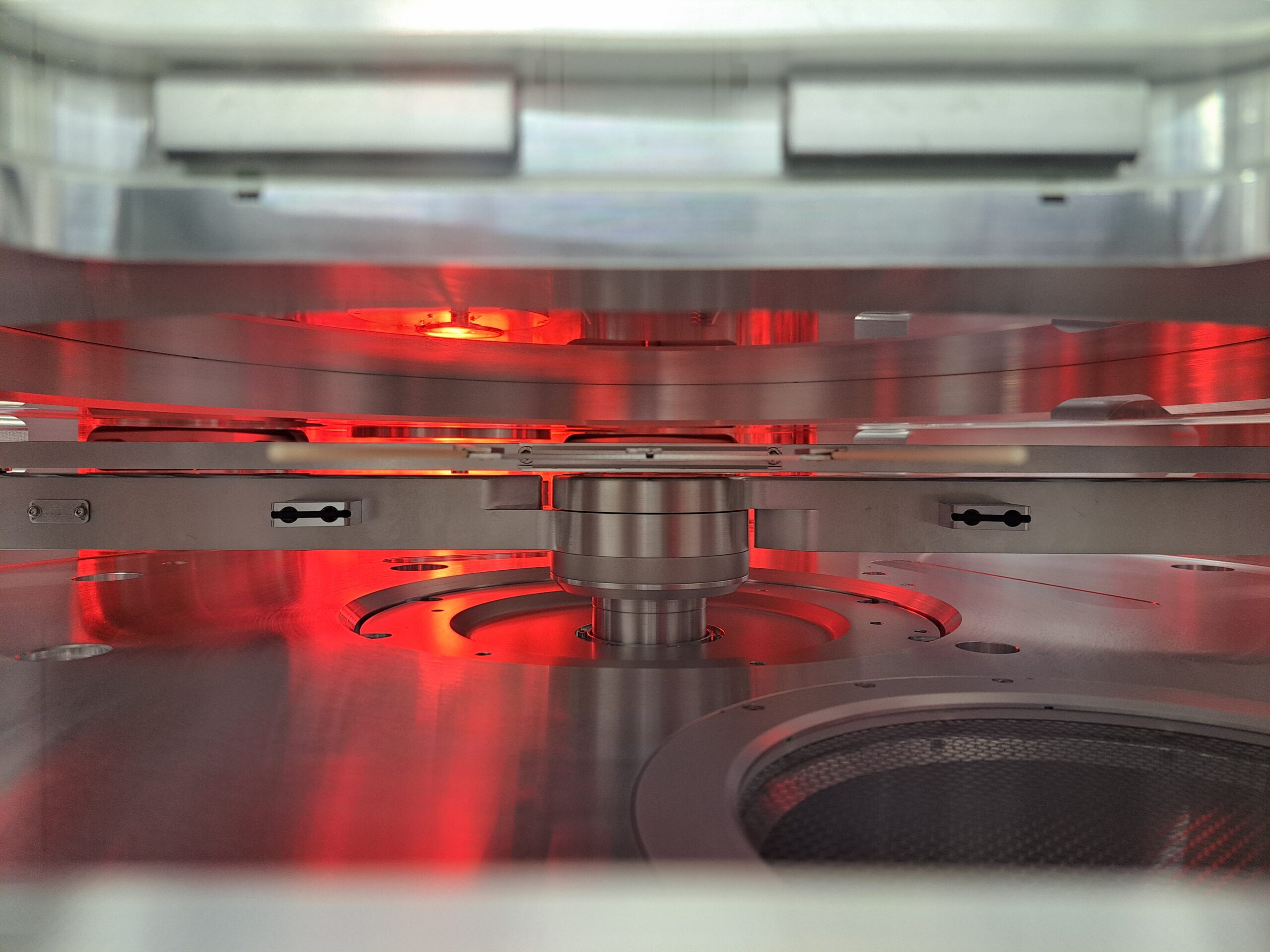
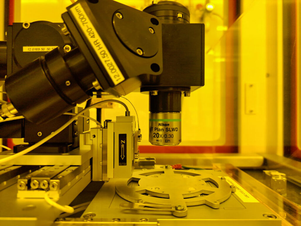
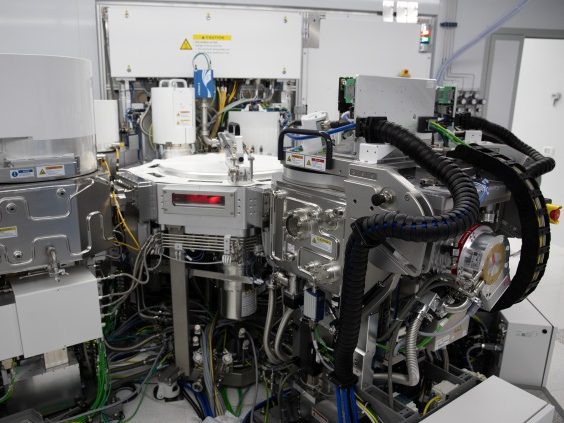
Polifab’s cleanroom includes an ISO 6 area of 330 m2 with facilities for optical lithography, electron beam lithography, wet and dry etching, thin film deposition and metrological characterization and an ISO 8 area of 290 m2 equipped with facilities for back-end, testing, thermal treatments and advanced depositions.
An additional non-cleanroom laboratory space 310 m2 provides advanced back-end, characterization and deposition tools for an even wider range of applications.
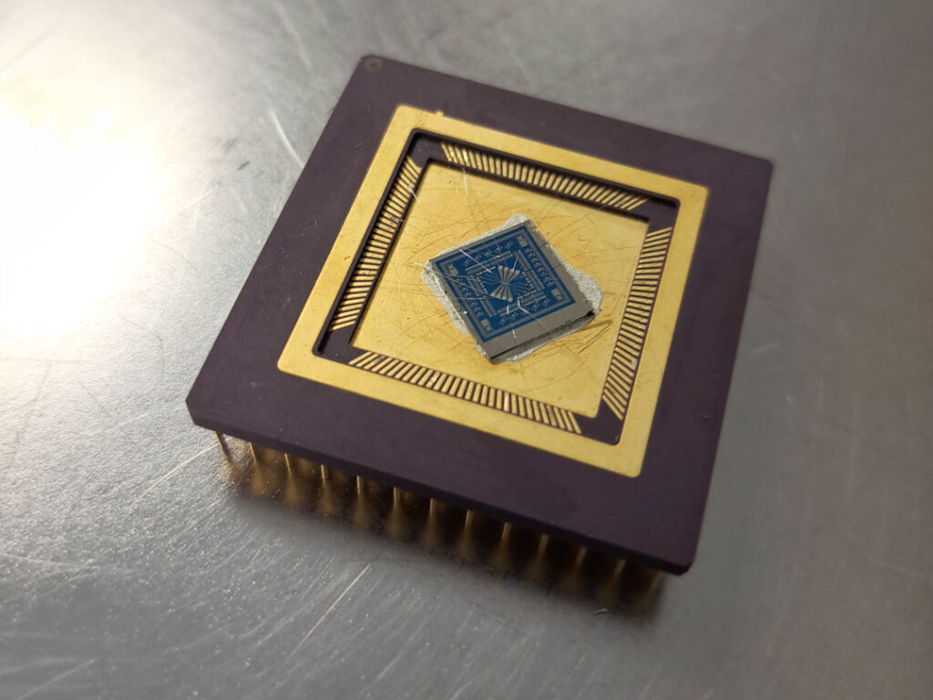
We can work on different substrate sizes from small samples up to 200 mm wafers and process several substrate materials such as silicon, glass, plastics, etc…
How do I interact with Polifab?
You can work with us either by directly accessing the cleanroom or by commissioning the fabrication/measurement to our staff.
In the first case you will be followed by our engineers who will introduce you the cleanroom and train you on the necessary tools: after this initial period, you will reserve your machine time via our dedicated booking system.
In the second case, the staff of Polifab will take care of your project, offering a third party service.
If you are interested, please check out our pricing list.
Let’s get in touch