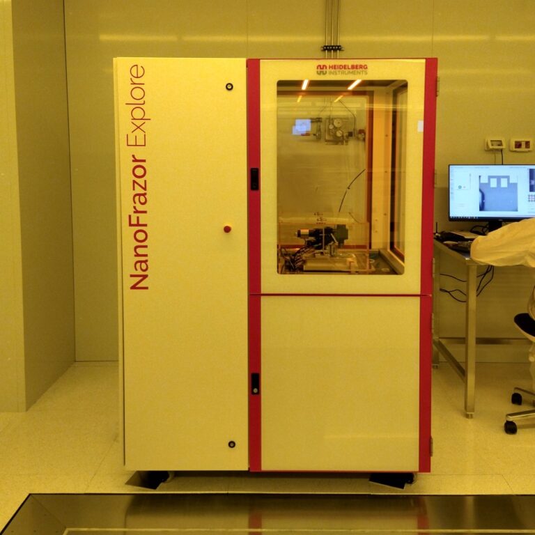
Description:
The NanoFrazor Explore is a nanofabrication tool based on Thermal Scanning Probe Lithography. Using an ultra-sharp heatable probe tip capable of both writing and imaging, it allows the creation of complex high-resolution nanostructures in a time efficient way: it represents an alternative to other expensive and complex direct-write methods like electron beam litography. It is also equipped with a laser writer module for speeding up the coarser patterning, so that both nano- and microfeatures can be quickly written on the same resist in a single fabrication step using the same software platform.
Working principle:
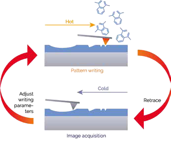
The heated probe tip creates arbitrary, high-resolution nanostructures by local sublimation of thermally sensitive resists (mainly PPA). Standard pattern transfer methods like lift-off or etching can be applied. Typical usage:
- Laser writing: Fast direct resist sublimation for large-area patterning, e.g. contact wires and pads
- Thermal probe writing: High precision and high resolution for the critical parts of the nanodevice
- Metrology, inspection and alignment: In-situ high-speed AFM with the same tip before, during or after patterning. No wet development required as the resist is removed directly.
Features:
- Direct heated probe writing with resolution below 15 nm
- Direct laser sublimation below 1 µm resolution
- In-situ high speed AFM topography imaging
- Sample size up to 100 mm x 100 mm
- Grayscale patterning with resolution and accuracy below 2 nm
- Markerless overlay and stitching using in-situ AFM for accurate alignment
- Superior acoustic and vibration isolation
- Enables numerous unique possibilities that go beyond conventional nanolithography