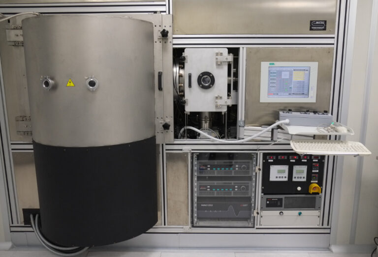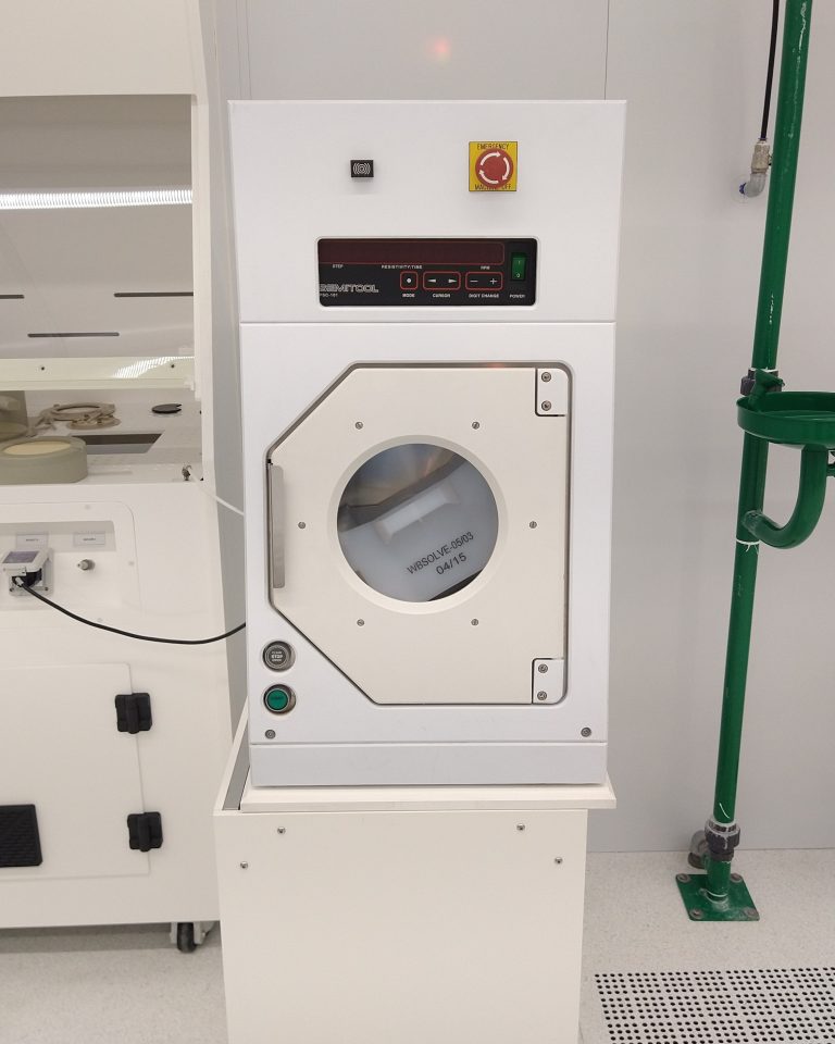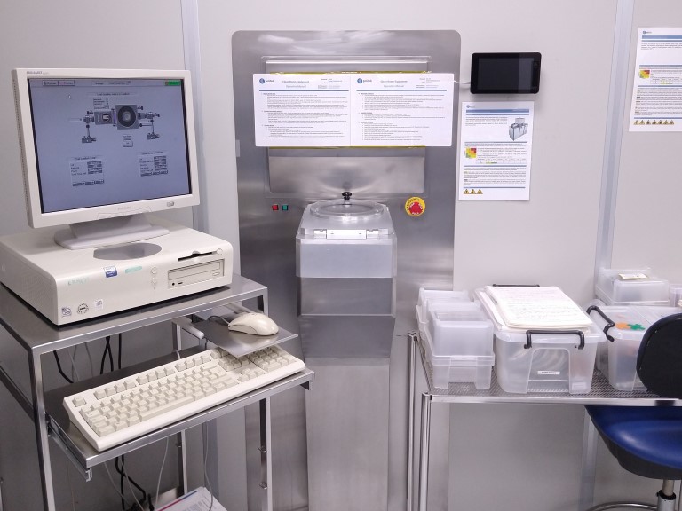
RIE ICP – Oxford Plasmalab 100
Details

Description:
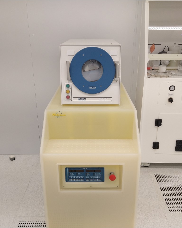
The Oxford Plasmalab 100 inductively coupled plasma (ICP) etcher is a multipurpose fluorocarbon based system that provides users anisotropic etching of silicon, silicon oxide, and other dielectric materials. The tool is equipped with a temperature controlled electrode to help users tailor their etch feature profiles. The manual load-lock system can accommodate substrates ranging from 200 mm diameter wafers down to small pieces.
Working principle
RIE uses chemically reactive plasma to remove material deposited on wafers. The plasma is generated under low pressure (vacuum) by an electromagnetic field. High-energy ions from the plasma attack the wafer surface and react with it. In ICP type of system, the plasma is generated with an RF powered magnetic field. Very high plasma densities can be achieved, though etch profiles tend to be more isotropic.
- High etch rates are achieved by high ion density (>1011 cm3) and high radical density
- Control over selectivity and damage is achieved by low ion energy
- Separate RF and ICP generators provide separate control over ion energy and ion density, enabling high process flexibility
- Low pressure processing yet still high density for improved profile control Chemical and ion-induced etching
- Can also be run in RIE mode for certain low etch rate applications
- High conductance pumping port provides high gas throughput for fastest etch rates
- Electrostatic shield eliminates capacitive coupling, reduces electrical damage to devices, reduces chamber particles
- Wafer clamping and helium cooling as standard, providing excellent temperature control with the option of a wide temperature range
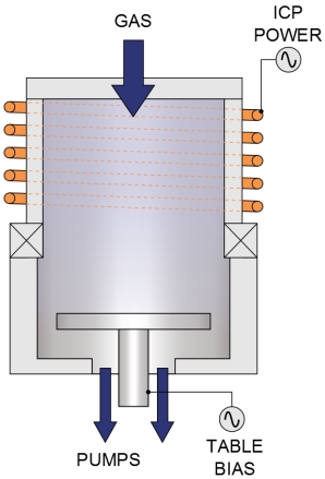
Schematic of the ICP RIE reaction chamber
Specifications
- Inductively coupled plasma (ICP) power source: up to 2500 W at 2.4 MHz.
- Radio frequency (RF) power source: up to 600 W at 13.56 MHz.
- Electrode temperature range: -150 °C to 300 °C.
- Unique process gases: octafluorocyclobutane (C4F8), trifluormethane (CHF3), and Sulfur Exafluoride (SF6).
- Anisotropic etching of silicon and silicon oxide.
- Low temperature silicon etching.
Supported Sample Sizes:
- Maximum wafer diameter: 200 mm (8 in).
- Wafer diameters: 75 mm (3 in), 100 mm (4 in) – default, 150 mm (6 in), and 200 mm (8 in).
- Small pieces supported: Yes.
Typical Applications:
- Silicon and silicon oxide stack etching.
- Optical device fabrication.
- General device patterning.

