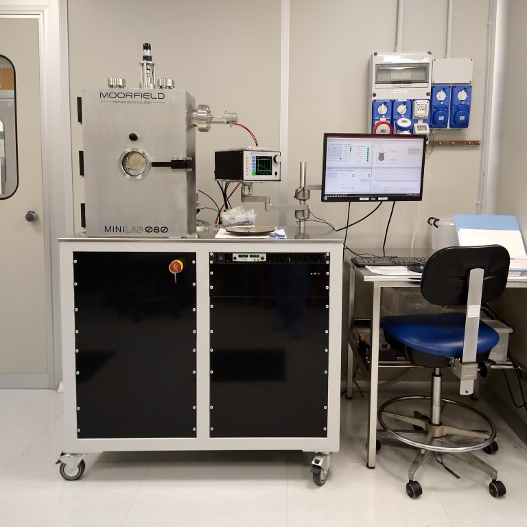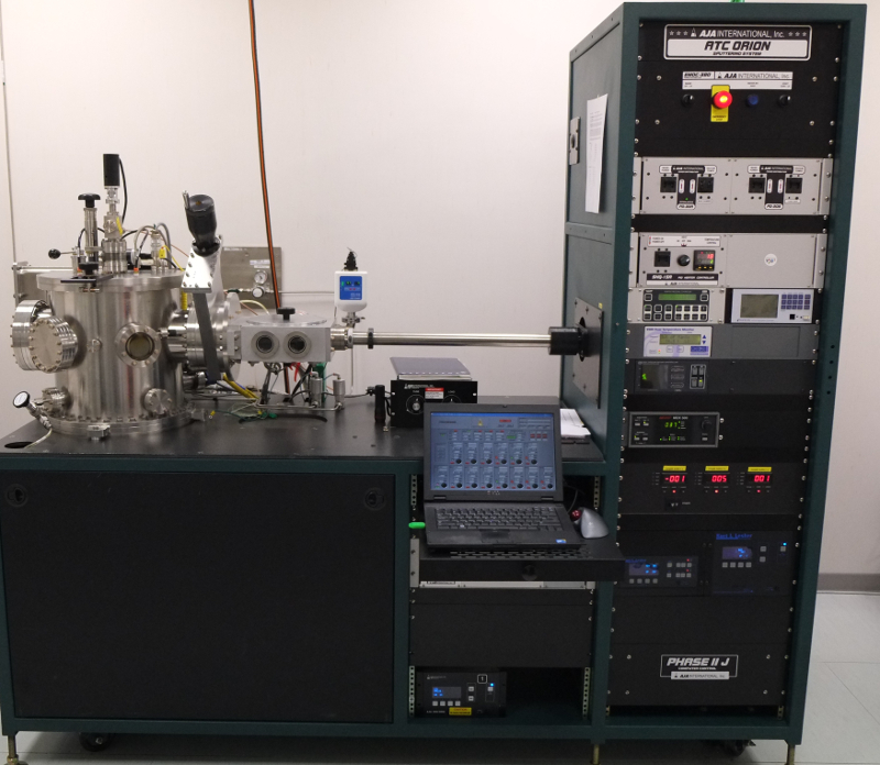
Sputtering System – AJA ATC Orion 8
Details

Description:
Equipment for deposition of thin films using magnetron sputtering on 3” substrates. Typical use: tunnel junction multilayer fabrication and dielectric materials deposition. The AJA system is provided with ten 2”/1”, DC and/or RF, magnetron sputtering sources, which are arranged in a confocal, sputtering-up configuration. The system allows to deposit multilayer structures with precise and automatic control of film thickness.
Working principle
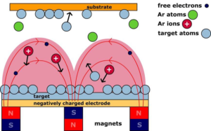
Magnetron sputtering is a physical vapor deposition technique, which allows a good film adhesion to the substrate, and a high control on the thickness, uniformity and composition of the deposited material. By first creating a gaseous plasma and then accelerating the ions from this plasma into some source material (a.k.a. “target”), the source material is eroded by the arriving ions via energy transfer and is ejected in the form of neutral particles – either individual atoms, clusters of atoms or molecules. As these neutral particles are ejected, they will travel in a straight line unless they come into contact with something – other particles or a nearby surface. If a “substrate” such as a Si wafer is placed in the path of these ejected particles, it will be coated by a thin film of the source material. In order to create the plasma, atoms of an inert gas (frequently Ar) are introduced into the HV (High Vacuum) chamber and a negative bias voltage is applied to the target. Free electron are immediately accelerated by the electron field in proximity to the target and ionize by collision the Ar atoms leaving Ar+ ions. This cascade process ignites the plasma. At this point, positively charged Ar+ ions are accelerated towards the negatively biased electrode, striking the surface and releasing source material and more free electrons by energy transfer. In magnetron sputtering, permanent magnets are located behind the target in order to confine the free electrons in a magnetic field directly above the target surface. This provides a double advantage: first, the free electrons, which are rejected by the negatively charged target, are prevented from bombarding the substrate, which would cause overheating and structural damage; second, the circuitous path carved by the free electrons along the lines of the magnetic field enhances the probability of ionizing neutral Ar atoms by several orders of magnitude. This increase in available ions significantly increases the rate at which target material is eroded and subsequently deposited onto the substrate.
Specifications
- 7 2” magnetron sputtering sources (A320-XP) with flip-top shutter.
- Thickness uniformity of ± 2% over 3” wafers.
- 3 1” magnetron sputtering sources (A310-XP) with sliding shutter.
- Sputter-up cluster flange.
- Confocal configuration.
- RF/DC operation capability.
- The magnet array can be configured by the customer to operate in the balanced, unbalanced and magnetic material modes.
- Motorized, rotating substrate holder for 3” substrates with in-situ manual Z motion.
- Substrate holder featuring reactive gas injection rings, RF bias capability.
- Substrate heater up to 800 °C.
- Magnetic sample holder.
- AJA Labview based Phase II-J computer control system.
- Possibility to operate in manual mode or in fully automated mode.
- Automatic closed-loop pressure control.
- Cryo Vacuum Pumping in the main chamber (base pressure 3*10-9 Torr).
- Load-lock system with a turbo-pump.